
Potting and Encapsulation
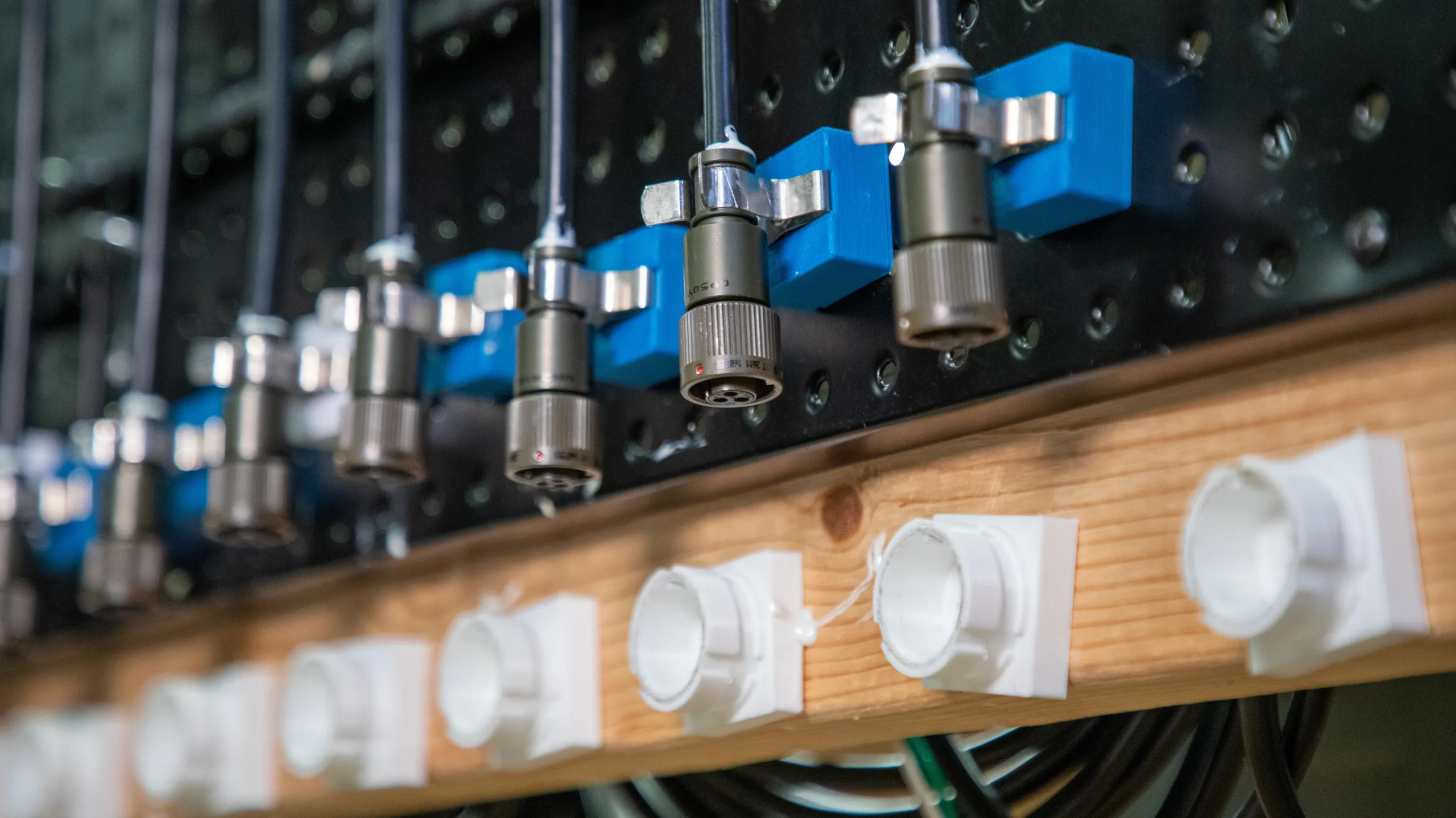
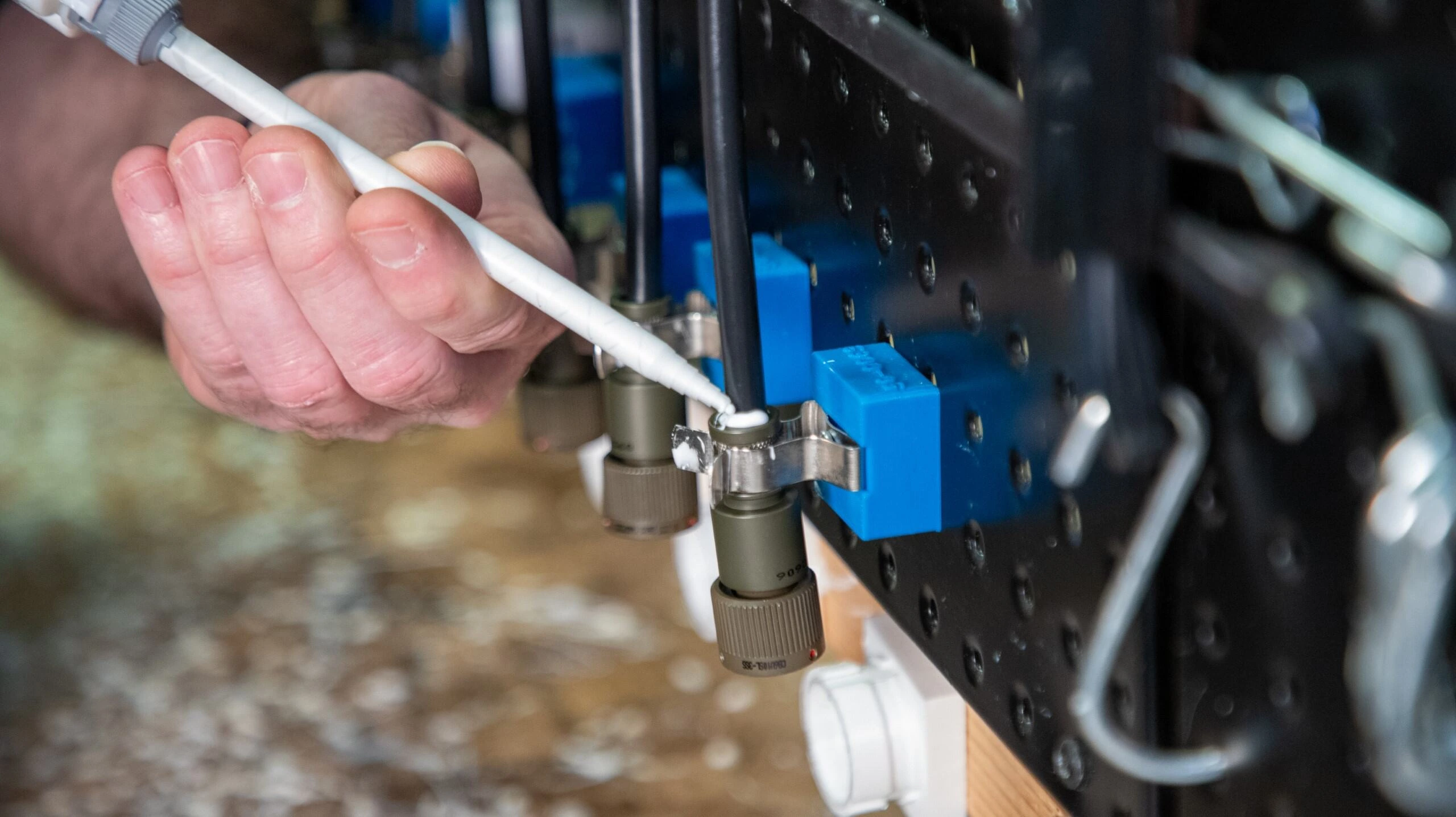
Electronic circuits and connector transitions in industrial equipment are vulnerable
to moisture ingress, vibration fatigue, and strain at critical connection points. Left unprotected, these stressors can cause intermittent signal loss or premature
field failures.
MJM Industries offers potting and electronic encapsulation services engineered to seal out environmental exposure and reinforce durability without compromising delicate circuits, connectors, or internal assemblies. Because every application is different, our team develops custom solutions aligned with unique design and performance requirements.
Potting vs Encapsulation
Potting and encapsulation integrate environmental protection directly into the assembly, eliminating the need for secondary sealing steps. The right choice depends on expected environmental exposure, required flexibility, and production volume.
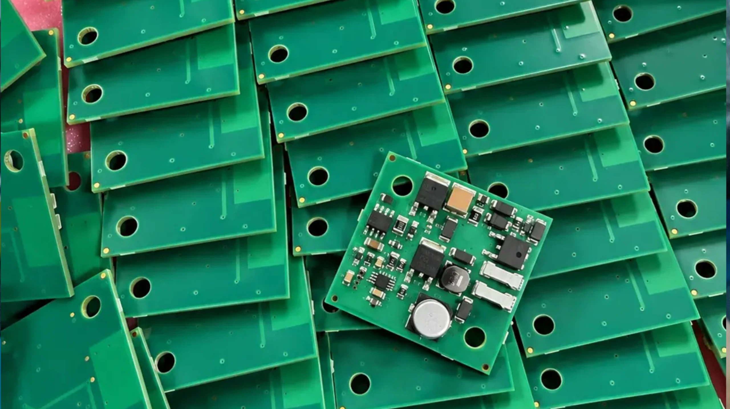
Potting
Potting is a manual, two-part process that mixes a resin, such as epoxy, polyurethane, or silicone, and a hardener to form a protective compound. The mixture is poured into a cavity or enclosure that surrounds the electronics, then cured into a rigid or semi-rigid mass.
The potting process requires precise mixing, controlled pouring, and longer cure times. Potting is commonly used for prototype validation, small-batch PCB assemblies and enclosed control boards where tooling for automated dispensing is not required.
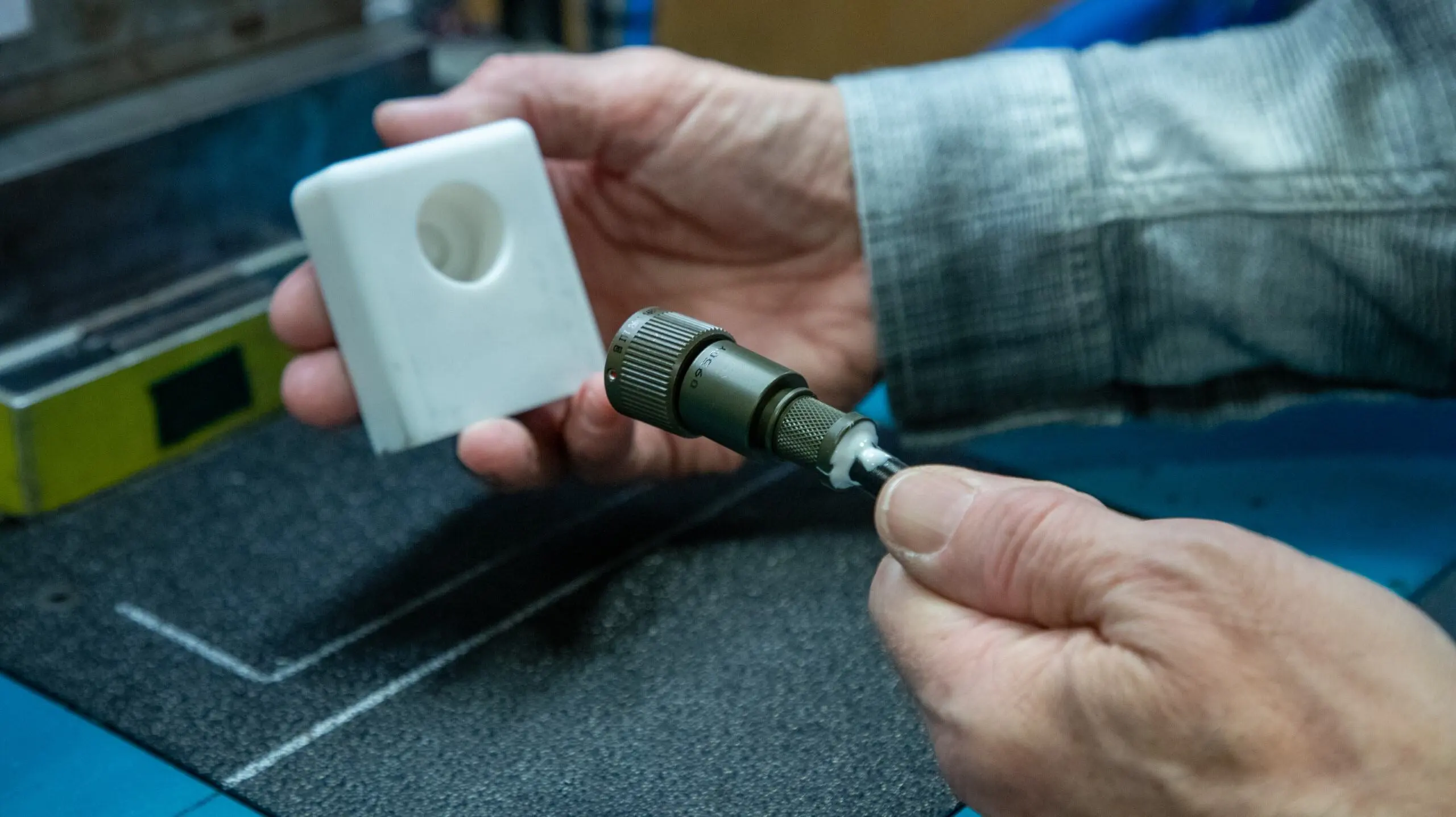
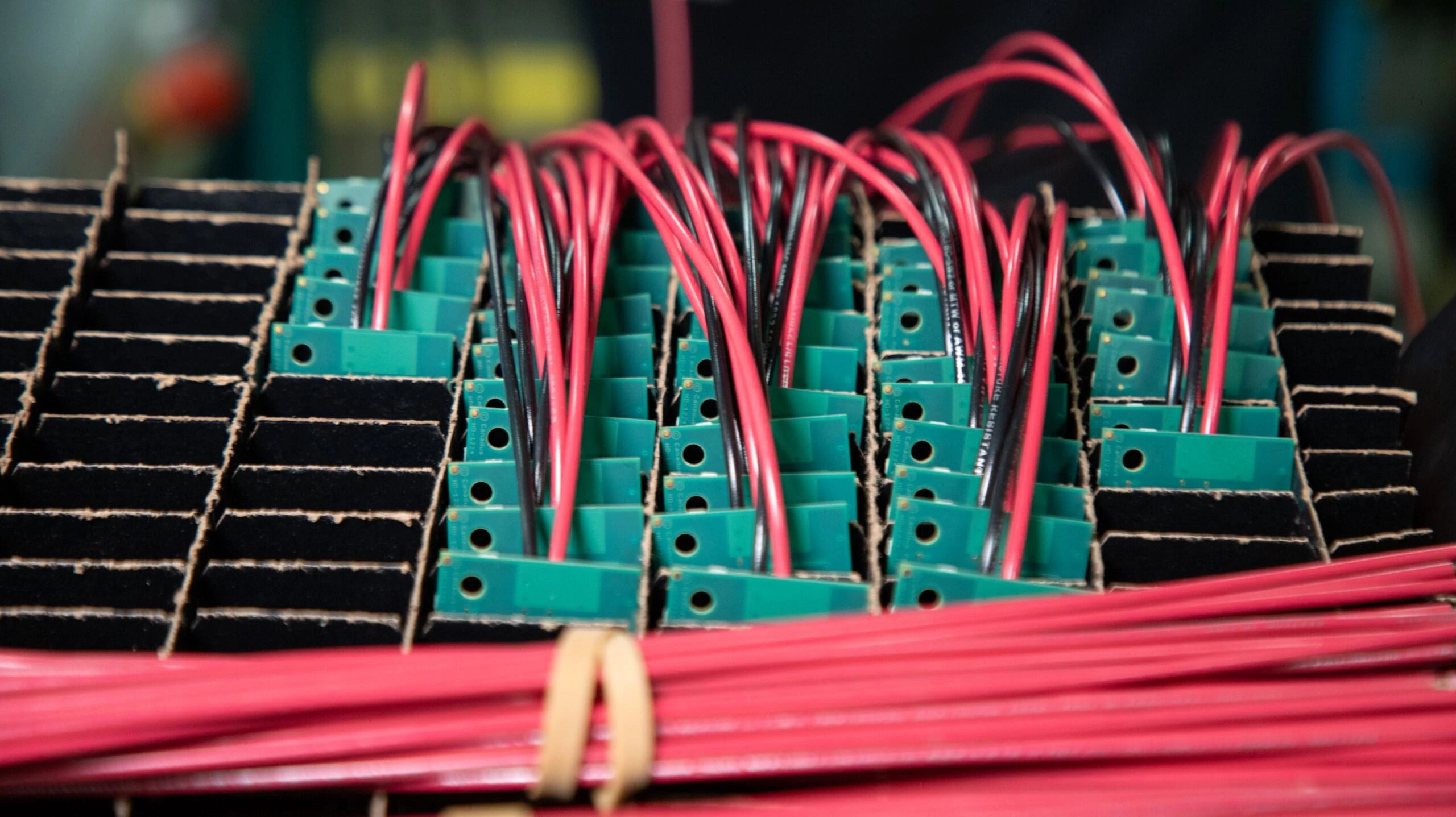
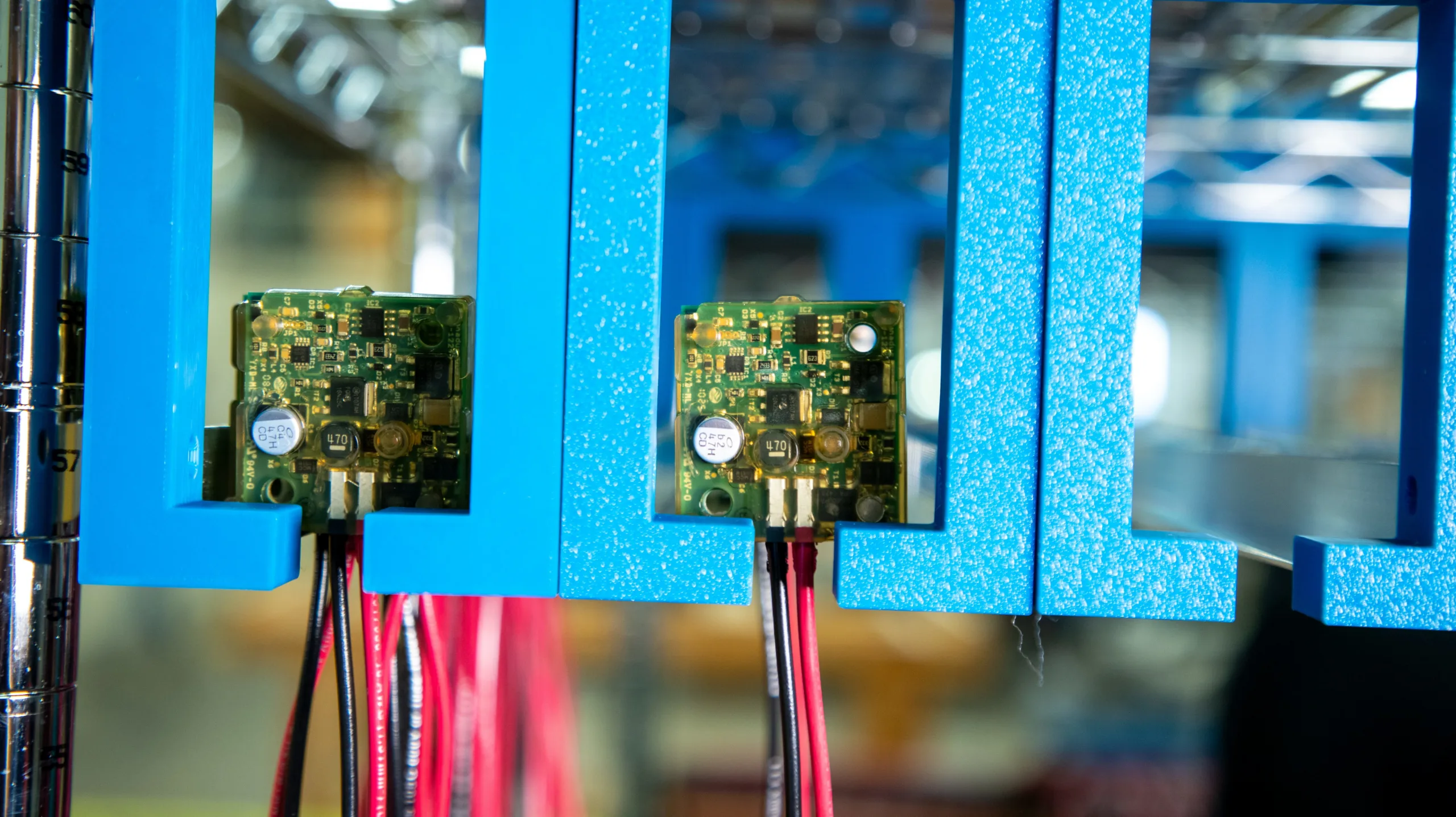
Encapsulation
Electronics encapsulation, such as conformal coating, uses low-viscosity compounds that flow around components and cure into a protective layer. Once cured, the material forms a durable barrier around cables, connectors, and PCBs, shielding internal parts while maintaining electrical integrity.
Encapsulation is ideal for delicate assemblies that require environmental sealing while preserving component stability and performance.
| Technical Factor | Potting | Encapsulation |
|---|---|---|
| Coverage Level | Compound fills entire cavity, fully embedding the electronics inside a solid protective mass | Compound forms protective layer around components without filling the entire housing or cavity |
| Environmental Protection | Very high protection against moisture, dust, chemicals, and vibration because the entire assembly is sealed | Moderate to high protection focused on critical components and connection points |
| Thermal Behavior | Heat distributed throughout the compound when thermally conductive materials are used, reducing localized hotspots | Heat transfer mainly in coated areas, may require additional thermal management in dense assemblies |
| Material Volume / Weight Impact | Higher material usage – entire cavity is filled, significantly increasing assembly weight | Lower material usage – only targeted areas are coated, resulting in a lighter assembly |
| Repairability / Serviceability | Once cured, components are difficult or impossible to access without destroying the assembly | Limited serviceability possible depending on encapsulation method and component accessibility |
| Material Consumption & Cost |
Higher compound volume and longer cure cycles, typically resulting in higher material and processing costs | Lower material consumption and faster processing, reducing overall production costs |
| IP Protection Potential | Capable of achieving very high ingress protection ratings depending on materials and design | Typically provides moderate to high ingress protection depending on coating thickness and coverage |
| Processing Time | Longer curing times and controlled processing conditions due to thicker material layers | Faster curing and quicker processing cycles due to thinner protective layers |
| Protection Against Reverse Engineering | Very high – internal circuitry and layout completely concealed within the cured compound | Partial visibility possible depending on coverage, making reverse engineering somewhat easier |
| Typical Applications | Power modules, control boards, high-vibration sensors, outdoor electronics, underwater equipment, and sealed industrial devices | Sensor modules, connector transitions, PCB assemblies, compact electronics, and applications requiring targeted protection |
Why Choose MJM Industries
MJM Industries supports potting and encapsulation programs with a hands-on, engineering-driven approach.
- In-house engineering, tooling, process expertise, and U.S.-based manufacturing with collaborative support from concept through production
- 100% testing where applicable
- Potted and encapsulated assemblies built to defined performance requirements
- Guidance on selecting PCB potting or encapsulation based on design and volume needs
With MJM Industries, you get responsive communication and a team approach for dependable, production-ready assemblies.